
- All
- Product Name
- Product Keyword
- Product Model
- Product Summary
- Product Description
- Multi Field Search

Views: 0 Author: Site Editor Publish Time: 2025-10-26 Origin: Site


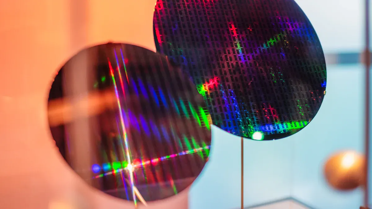
Silicon wafers are used the most in electronics in 2025. They are cheap and work in many ways, like in CPUs and memory chips.
Silicon carbide wafers work well with lots of power and heat. This makes them good for electric cars and power electronics.
Gallium arsenide and indium phosphide wafers are best for fast jobs, like telecom and photonics. But they cost more and do not last as long.
Silicon wafers are used in most electronics today. They have good semiconductor properties and can handle heat well. People use silicon wafers for advanced chips and AI. They are also used in computers that need to work fast. Big industries like cars and factories use large 300mm silicon wafers. These bigger wafers help things run better. Silicon wafers are found in memory chips and stacked chips too.
Silicon carbide wafers work great in power electronics. They can handle high voltages and heat easily. These wafers cost more than silicon ones. But they are more efficient and reliable. You see silicon carbide wafers in electric cars and green energy systems. They are chosen when power and strength are important.
Gallium arsenide wafers help devices run very fast. They are used in telecom and optoelectronics. These wafers let electrons move quickly and have a direct bandgap. This makes them good for RF and microwave devices. Gallium arsenide wafers reach higher frequencies than silicon. But they break more easily and cost more. So, people use them only for special jobs.
Indium phosphide wafers are best for photonic and fast data devices. They let electrons move quickly and have great optical features. These wafers are used in lasers and fast data chips. Indium phosphide wafers work well in advanced photonic circuits. They stay stable even when temperatures change a lot.
Sapphire wafers are very hard and can handle heat. They are used as bases for LEDs in lights and screens. Sapphire wafers also help in RF devices and protect windows in tough places. Their scratch resistance is good for medical and science tools.
New wafer materials like gallium nitride, graphene, and molybdenum disulfide are becoming popular. These wafers help electronics use less power and work better. Some, like ferroelectric and memristive wafers, are used in AI and brain-like computing. These new wafers can be expensive and hard to make. But they offer many new chances for the future.
When you pick a wafer, you must think about electricity and heat. Each wafer material acts in its own way. Some wafers let electrons move really fast. Some can handle high heat without breaking. Here is a table that shows how some wafer materials compare:
Material | Bandgap (eV) | Electron Mobility | Thermal Conductivity | Key Applications |
|---|---|---|---|---|
Silicon | 1.12 | Moderate | Good | CPUs, GPUs, Memory, Solar cells |
Silicon Carbide | Wide | Moderate | Excellent | Power electronics, Electric vehicles |
Gallium Arsenide | Direct | High | Moderate | RF, Microwave, Optoelectronics |
Indium Phosphide | Direct | High | Good | Fiber optics, Laser technology |
Sapphire | Insulator | N/A | High | LEDs, RF, Protective windows |
Silicon wafers are good for most chips. Silicon carbide wafers are better with heat and power. Gallium arsenide wafers help with fast-moving electrons. Indium phosphide wafers are great for lasers and fiber optics. Sapphire wafers do not carry electricity but are tough in hard places.
GaAs wafers are III-V direct bandgap semiconductors. They are great for optoelectronic devices. Their high electron mobility and direct bandgap help with light. This makes them good for things like solar cells and laser diodes.
Mechanical strength means how tough a wafer is. Cost is important when you pick a wafer. Some wafers are strong but cost a lot. Some are cheaper but break more easily. This table shows how silicon carbide is different:
Property | Silicon Carbide (SiC) |
|---|---|
Fracture Toughness | High |
Tensile Strength | High |
Anisotropic Behavior | Yes |
Processing Techniques | Laser slicing |
Silicon carbide wafers are very strong and hard to break. They can be cut with lasers. Silicon wafers are not as tough but cost less. Gallium arsenide wafers break more and cost more. Indium phosphide wafers are also easy to break and expensive. Sapphire wafers are hard and do not scratch, but they cost more.
Problems in the supply chain can change wafer prices. In 2025, prices for advanced wafers may go up. This is because of tariffs and more demand for AI chips. Some companies may raise prices by 10%. Making a chip in the US costs more than in Taiwan. These things can change which wafer you pick.
You must match the wafer to what you need. Here is a quick guide:
Silicon wafers: Good for CPUs, GPUs, memory, and most chips. They are easy to find and work well.
Silicon carbide wafers: Best for electric cars and power electronics. They last longer in hard places.
Gallium arsenide wafers: Great for high-frequency and optoelectronic devices. You find them in laser diodes and microwave circuits.
Indium phosphide wafers: Used in fiber optics and fast data chips.
Sapphire wafers: Used for LEDs, RF devices, and as covers.
The table below shows how each wafer fits key uses:
Wafer Type | Unique Properties | Key Applications |
|---|---|---|
Silicon | Moderate electron mobility, indirect bandgap | Logic circuits, microprocessors, solar cells |
Gallium Arsenide | High electron mobility, direct bandgap | RF devices, microwave amplifiers, optoelectronics |
Silicon Carbide | Excellent thermal conductivity, wide bandgap | Power electronics, electric vehicles, high-temperature environments |
Indium Phosphide | High electron mobility, direct bandgap | Fiber optics, laser technology |
When you make MEMS or solar cells, you must make choices. Some wafers cost less but are not as precise. Some wafers work better but cost more. Here is a table to help you see the differences:
Wafer Type | Advantages | Disadvantages |
|---|---|---|
SSP | Budget-friendly, suitable for bulk micromachining | Limited precision for advanced applications |
DSP | High precision for dual-sided processing | Higher cost than SSP |
Bonded SOI | Excellent for high-performance applications, electrical isolation | More expensive, requires specific applications |
E-SOI® | Tight device layer uniformity | Higher cost, niche applications |
C-SOI® | Reduces process steps, ideal for complex designs | More expensive, requires advanced design considerations |
Silicon wafers are still the most used in 2025. You see them in most chips because they are easy to make and cost less. Big 300mm silicon wafers help make lots of chips fast. This keeps prices down and supply steady. Governments help local silicon wafer makers, which keeps the market strong.
Factor | Description |
|---|---|
Technological Advancements | 300mm wafers offer economies of scale for high-volume manufacturing |
High Demand | Logic/MPU and Memory applications drive demand for high-purity silicon wafers |
Barriers to Entry | Complex manufacturing and high investment keep new suppliers out |
Government Support | Subsidies and initiatives boost local wafer production |
Market Concentration | Top five vendors control 82% of the market |
You may need other wafers for special jobs. Silicon carbide wafers are better for high-power and hot places. Gallium arsenide wafers are good for speed and light. Indium phosphide wafers are best for fiber optics. Sapphire wafers protect devices in tough places.
When you pick a wafer, think about how long it will last. Wafers with fewer defects last longer and work better. Good surface quality and strong crystals help your chip stay stable. If a wafer has many defects, your chip may break sooner.
The semiconductor industry uses a lot of energy and water. Making wafers can cause greenhouse gases and chemical waste. You should think about the environment when you pick a wafer. Newer ways try to use less energy and make less waste.
You also see new ways to make wafers. Fan-Out Wafer Level Packaging (FOWLP) helps make smaller, faster chips. Companies use new materials and better tools to check wafer quality. These changes help you get better chips for AI, 5G, and other new tech.
Pick wafer materials that match what you need. Silicon is good for most chips. Silicon carbide is used for power jobs. Gallium arsenide is best for fast devices. Think about electricity, strength, and price when you choose. New materials and 3D stacking will change electronics soon.
Silicon wafers are used the most. They work for many types of chips. They also cost less than other wafer materials.
Silicon carbide can take a lot of heat and high voltage.
It helps car electronics last longer and work better.
Some wafers can be recycled. ♻️ Silicon is often recycled. Other wafer materials need special steps and cost more to recycle.
