
- All
- Product Name
- Product Keyword
- Product Model
- Product Summary
- Product Description
- Multi Field Search

Views: 0 Author: Site Editor Publish Time: 2025-10-27 Origin: Site


Silicon wafers help control electrical signals. This lets your favorite apps work.
High thermal conductivity in these consumables stops your device from getting too hot.
Strong mechanical stability helps your gadgets work well for a long time.
Learning about consumables helps you see why some devices last longer and work better than others.
Wafer consumables are very important for gadgets to work well. They help control electricity, manage heat, and keep things stable.
Using good silicon wafers makes devices work better. Clean and smooth surfaces help gadgets run faster and more reliably.
Handling consumables the right way stops damage and keeps things clean. This helps devices last longer and need fewer repairs.
New wafer technology, like 3D chip stacking, makes devices work better. These new ideas help make gadgets smaller, faster, and use less energy.
Knowing about wafer consumables helps you choose better technology. Learning more gives you better gadgets.
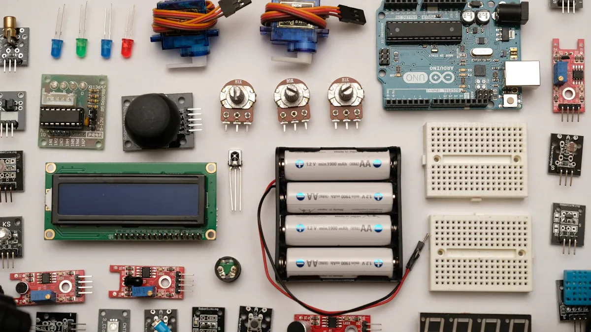
You use gadgets all the time, but you may not know what helps them work. Wafer consumables are supplies and tools that get used up when making electronic devices. These include wet chemicals for cleaning, special gloves for handling, and parts that help machines work well. Factories need these supplies to keep making good gadgets.
Tip: Wafer consumables matter because they help keep the process clean and exact. Clean supplies mean better gadgets for you.
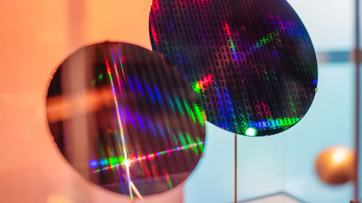
Silicon wafers are thin, round pieces of crystal. They are the base for building electronic parts. Factories use silicon wafers because they are very pure and have great semiconducting abilities. You can find silicon wafers in smartphones, TVs, and cars. In medical devices, they help with things like X-ray detectors and lab-on-a-chip tools.
There are many kinds of consumables in semiconductor manufacturing. Each one has a special job to do. Here are some common types:
Wet chemicals: Used to clean and etch wafers.
Handling consumables: Gloves, tweezers, and containers keep wafers safe from dirt and harm.
Equipment parts: Filters, seals, and other machine parts that need to be replaced often.
You also see different types of wafers used as consumables. The table below lists two main types:
Type of Wafer | Description |
|---|---|
Undoped Semiconductor Wafers | Thin slice of pure silicon crystal or another kind of semiconductor material. |
Doped Semiconductor Wafers | Made by adding other materials during making to control how they work. |
Other materials, like aluminum, help move electricity in circuits. Silicon is the main part used for most integrated circuits.
You are part of the tech world every time you use a device. Wafer consumables help factories make the chips inside your gadgets. The process starts with getting the wafer ready. Workers pick and clean a silicon wafer to make sure it is ready for building parts. They use wet chemicals to get rid of dirt or dust. Handling consumables, like gloves and special tools, keep the wafer safe from scratches.
Each step in making semiconductors uses different consumables. For example, equipment parts help machines add or take away layers on the wafer. Quality checks happen at every step to make sure the wafer is still good. If there is a problem, workers can fix it before moving on.
Silicon wafers are the base for electronics and medical devices. In electronics, they hold the tiny circuits that power your phone or computer. In medical devices, they help with things like imaging and checking health, such as in pacemakers or glucose monitors. You get better gadgets because of these consumables.
Note: Taking care of wafer consumables helps your devices work better and last longer.
You want your gadgets to work fast and not lag. The quality of consumables used in factories is very important. When factories use good materials, your devices can work faster and save energy. The wafer’s surface must be flat and clean. If there is dirt or damage, the tiny circuits might not work right. This can make your phone or tablet slow.
The quality of silicon wafers helps your devices work well.
Defect density, surface quality, and crystal structure are important for how your device works.
High defect density can cause more leakage current and less thermal stability.
If the surface is not flat or is dirty, it is hard to make small chip parts.
Defects can make devices wear out faster and need repairs sooner.
You can see how different materials help with speed and power. The table below shows some common materials and what they are used for:
Material | Key Properties | Primary Applications | Dicing Challenges | Recommended Blade & Setup |
|---|---|---|---|---|
Silicon (Si) | High purity, excellent structure | Integrated circuits, sensors | Thin wafers chip easily | SMART CUT® Nickel Bond; diamond size 4–6 µm; feed 40–75 mm/s |
Gallium Arsenide | High electron mobility | LEDs, RF amplifiers | Brittle, microcracks form easily | Nickel Bond blades; fine grit; low feed; strong coolant flush |
Silicon Carbide | Extremely hard, wide bandgap | Power electronics, EV inverters | Hard to cut, rapid blade wear | Nickel Bond, larger grit; moderate feed; high-pressure coolant |
When you use a device made with good consumables, it is faster, sounds better, and the battery lasts longer.
You want your gadgets to last a long time. The quality of consumables used in making them helps with this. If factories use the best materials and tools, your devices can handle daily use and last longer. Wafer-level reliability testing checks for problems before you get the device. Better manufacturing at every step makes devices more reliable. This means your phone or laptop is less likely to break or stop working early.
There is a strong link between consumable quality and device failure rates. In medical devices, using expert-level quality management helps stop failures. This keeps devices safe and working well for a long time. You will have fewer repairs and replacements.
Note: Good consumables mean your gadgets break less and last longer.
You see new features in gadgets every year. Better consumables help make these new features possible. Factories now use flexible wafer shapes, like rectangles, to fit more chips in small spaces. This lets your devices do more but stay small and light.
Flexible design: Rectangular wafers allow for new shapes and better integration.
Enhanced performance: High-quality surfaces and better electrical properties make devices more reliable and use less power.
Material utilization: New wafer shapes help reduce waste and improve energy conversion, especially in solar cells.
When factories use better consumables, they can make faster, smarter, and more energy-efficient devices. You get to use the newest technology because of these changes.
Factories use wet chemicals at every step of making wafers. These chemicals clean and shape the wafer’s surface. They remove tiny bits of dirt and help make patterns. Photoresist chemicals are part of this group. They cover the wafer and help form circuit designs. Photoresist chemicals change when exposed to light. This lets workers make very exact patterns. Strong cleaners keep the wafer pure. Photoresist chemicals also block changes in certain areas. These chemicals are important for making chips smaller and faster.
Tip: Using clean wet chemicals and photoresist chemicals helps your devices work well and last longer.
Workers must be careful when touching wafers in factories. Handling consumables are things like carriers, tweezers, and gloves. Tweezers help pick up and move wafers safely. The tips of tweezers help line up wafers just right. Gloves and carriers keep wafers clean. These tools stop dirt and damage. Workers use them in cleanrooms with strict rules.
Wafer tweezers help stop drops, scratches, and dirt.
Special tips help line up wafers during work.
Tweezers keep things clean in special rooms.
Cleanroom tools keep wafers free from dust.
Careful handling with the right tools makes more good chips. You get better gadgets because factories use these tools.
Machines need equipment consumables to work well. These include filters, seals, and blades. Blades cut wafers into small pieces. Filters keep air and chemicals clean. Seals stop leaks and protect parts. Workers change these parts often to stop problems. Clean machines help photoresist chemicals work better. Good equipment consumables help make more chips with fewer mistakes.
Equipment Consumable | Purpose | Impact on Wafer Quality |
|---|---|---|
Filters | Remove particles | Cleaner wafer surfaces |
Blades | Cut wafers | Precise chip shapes |
Seals | Prevent leaks | Stable processing environment |
Every consumable, from photoresist chemicals to handling tools, helps make strong and high-quality devices.
Factories pick consumables very carefully. They want your gadgets to be strong and last long. Workers check if each consumable can handle chemicals, heat, and rough use. This keeps the wafer safe while it is made. It also helps the final product stay strong.
Here is a table that shows what factories look for when choosing consumables:
Criteria | Description |
|---|---|
Chemical Resistance | Stops contamination from acids, bases, and solvents used in making. |
Thermal Stability | Keeps shape at high heat, stopping damage from getting too hot. |
Mechanical Strength | Makes sure carriers can move wafers without breaking or bending. |
Factories test consumables at every step. They track how long each consumable lasts. Good management means your devices work better and last longer.
When factories manage consumables well, your gadgets get better. Devices break less, work faster, and cost less over time. You do not have to replace them as often.
Here are some ways good management helps you:
You get gadgets with fewer problems.
Devices last longer, so you save money.
Companies spend less, which can lower prices for you.
The table below shows how good management gives you real benefits:
Benefit Description | Measurable Impact |
|---|---|
Reduced stock-outs and expirables | Keeps supplies ready, stops delays, and cuts waste from expired items. |
Improved operational efficiency | Saves time, less manual work, and helps teams work together. |
Audit-ready inventory planning | Makes sure companies follow rules and keep records, so audits are easy. |
Financial control and cost savings | Cuts extra inventory and lowers costs, freeing money for new projects. |
You can trust that good consumables management helps your devices from start to finish. This focus on quality and cost means you get better gadgets every day.
Every year, new trends appear in wafer consumables. Factories now use machine learning to control processes. This helps them use materials better and make improved chips. Multi-patterning lithography helps make chips smaller and faster. Factories also stack chips on top of each other. This is called 3D chip stacking. It saves space and makes devices work better.
Many factories try to help the environment. They use less waste and follow new rules. Digital tools and automation help track every consumable. This makes work quicker and more dependable.
Here is a table with some new trends:
Trend/Technology | Description |
|---|---|
Wet Chemicals | Used for cleaning and etching, ensuring high-quality semiconductor devices. |
Advanced Node Technologies | Moves to 2-nanometer chips, needing better materials and usage control. |
Miniaturization | Smaller chips mean faster processing and less energy usage. |
3D Chip Stacking | Stacks components vertically, improving usage of space and performance. |
AI-Centric Processors | Smarter chips for real-time tasks, expanding the usage of semiconductors. |
Tip: These new ideas help you when you use a new phone or smart device.
You will see even more changes soon. Experts think factories will use silicon photonics for faster data. This will help your devices use data better and move it faster. New memory, like HBM and GDDR7, will help your devices store more. Liquid cooling systems will keep powerful computers from getting too hot.
AI will help factories find and use new materials. You will see more wide band gap semiconductors, like silicon carbide and gallium nitride. These help devices use power and heat better. Factories will also use greener materials and cleaner energy.
Asia-Pacific countries, like India and China, will grow fast in this field. They will lead in using new semiconductor technologies. AI will help find new materials, so devices will get faster and smarter.
AI helps find and use new materials.
New materials like 2D materials and quantum dots will change semiconductors.
Factories will use more digital tools to track and improve quality.
Note: The future of semiconductor consumables depends on smarter use, better materials, and new ideas from around the world.
You have learned that wafer consumables are important for your gadgets.
Cleaning and checking wafers helps devices work well.
Clean materials keep chips safe from tiny bits that cause trouble.
Good packaging protects chips, so your devices last longer.
When you know more about these materials, you want smaller and faster devices. If you care about the technology inside your gadgets, you can make better choices.
A wafer has three main parts. These are the edge, the flat surface, and the thin body. The edge helps workers hold the wafer safely. The flat surface is where circuits are built. The thin body gives support to the whole wafer.
Good management makes consumables better. Workers watch inventory and track how much is used. Real-time tracking helps control what is happening. Each consumable is checked during making. This keeps inventory correct and cuts down on waste.
Tracking and monitoring help you control consumables. You can find problems early. Real-time tracking shows what is in stock. Usage tracking tells you when to order more. This stops shortages and keeps factories working.
There are some challenges with consumables management. It is hard to keep inventory numbers right. Reordering can be tricky. You must watch costs and stop waste. Every item needs to be tracked. You need enough for making devices. Monitoring helps fix these problems.
Inventory checks and usage tracking tell you when to reorder. Control systems help with reordering. Workers check the consumables’ life cycle. They make sure supplies do not run out. This keeps the process smooth and devices high quality.
