


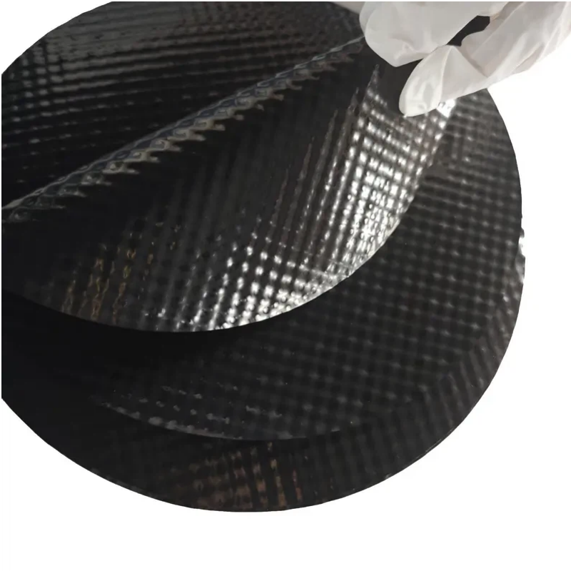
What is ESD Wafer Pads
Haouger Tech’s ESD wafer pads are engineered to protect semiconductor, solar, and glass wafers during separation, handling, storage, and transport. Made from high-purity PE or PS with permanent anti-static treatment, they effectively prevent static buildup, particle contamination, and surface scratches. The pads feature smooth or embossed textures for stable cushioning and shock absorption, ensuring wafers remain secure in trays, carriers, and shipping boxes. Cleanroom-ready and non-dusting, each pad offers consistent surface resistance and long-term reliability. Haouger Tech provides full customization in size, shape, thickness, and patterns for 6", 8", 12", and non-standard wafer applications.
Key Features of Haouger Tech ESD Wafer Pads
Permanent Anti-Static Protection
Engineered with durable ESD-treated PE or PS materials, the pads maintain stable surface resistance to prevent static buildup, safeguarding wafers from electrostatic discharge and particle attraction during handling.
Superior Scratch and Damage Prevention
Smooth or embossed surfaces provide controlled contact, reducing friction, scratches, and wafer edge chipping while ensuring safe separation and transportation in trays, cassettes, and carriers.
Cleanroom-Ready, Non-Dusting Performance
Manufactured with low-particle materials, the pads ensure a clean surface that does not shed, degrade, or contaminate sensitive semiconductor wafers during storage or movement in controlled environments.
Full Customization for Wafer Compatibility
Available in custom sizes, thicknesses, shapes, and patterns, the pads fit 6", 8", 12", and non-standard wafers, providing tailored mechanical support and optimized protection for diverse equipment and packaging formats.
Application
ESD wafer pads are widely used across semiconductor, solar, and precision glass manufacturing to protect wafers during storage, transport, and handling. Their anti-static, cushioning, and non-dusting properties ensure wafer integrity throughout cleanroom operations and packaging workflows.

Semiconductor Wafer Handling
Used in wafer fabs to protect 6", 8", and 12" IC wafers during loading, unloading, sorting, and manual or robotic transfer. The pads prevent electrostatic discharge, surface scratches, and chipping, ensuring safe handling throughout front-end and back-end semiconductor manufacturing processes.
Solar Cell and PV Wafer Packaging
Applied in solar wafer trays and shipping boxes, the pads secure mono-crystalline and poly-crystalline wafers during mass transportation. They minimize vibration, prevent micro-cracks, and reduce contamination risks, supporting high yield and safe logistics for photovoltaic manufacturing lines.


Glass, TFT, and Micro-LED Wafer Protection
Ideal for fragile glass wafers, TFT substrates, and Micro-LED panels, the pads provide stable separation and cushioning inside carriers. Their clean, non-dusting surfaces prevent particle contamination while maintaining dimensional stability during inspection, storage, and short-distance transport.
Product Advantages
Stable Anti-Static Performance
Engineered with permanent ESD materials, the pads maintain consistent surface resistance to prevent static buildup, ensuring reliable wafer protection throughout handling, packaging, and cleanroom operations.
Clean, Non-Dusting, and Safe for Wafers
Made from high-purity PE or PS, the pads do not shed particles or residues, preventing contamination and keeping semiconductor, solar, and glass wafers clean and protected.
Enhanced Cushioning and Scratch Prevention
Smooth or embossed textures offer controlled padding that reduces friction, absorbs shock, and prevents wafer edge chipping during movement, transport, or stacking in trays and carriers.
Full Customization for Multiple Wafer Sizes
Available in customized shapes, thicknesses, and patterns, the pads fit 6", 8", 12", and non-standard wafers, providing tailored compatibility for diverse equipment, packaging systems, and production lines.
Resource
- Name
- Update
- Size
- Downloads
- Thumbnail
- Download
- Copy Link
- 2-01-TDS-JH5063 wafer seperator.pdf
- 2025-10-29
- 447KB
- 35
-

- Download
- Copy Link

- TDS-JH8000 PU conductive film.pdf
- 2025-10-28
- 430KB
- 39
-

- Download
- Copy Link

- TDS-JH800S conductive silver film.pdf
- 2025-10-27
- 377KB
- 32
-

- Download
- Copy Link

- TDS-JH7000 PE conductive film.pdf
- 2025-09-26
- 375KB
- 24
-
- Download
- Copy Link
- HAOUGER.pdf
- 2025-09-26
- 12.08MB
- 34
-
- Download
- Copy Link
- 1-05-TDS-JH6000 composite conductive film.pdf
- 2025-09-24
- 417KB
- 27
-
- Download
- Copy Link
Company Advantage(Why choose us)
High-purity ESD wafer pads ensuring clean, safe, and stable protection.
Advanced Material Engineering
Expert in conductive films and ESD materials, delivering reliable, high-performance solutions for semiconductor and precision manufacturing industries.
Strong Customization Capability
Provides flexible customization in size, thickness, patterns, and resistance values to meet diverse wafer handling and packaging requirements.
Strict Quality and Cleanroom Standards

Related Product


FAQs
Contact Us
Related Blogs
-
 In the solar energy industry, ensuring the highest quality of solar cells is essential for producing durable, high-efficiency products.News
 -
 The solar energy industry has seen rapid growth in recent years, with solar power becoming one of the most important sources of renewable energy worldwide.News
 -
 In the high-tech manufacturing world, especially in the production of solar cells and TFT-LCD panels, the handling and transport of wafers are crucial processes.News


Keep in Touch With Us
Get in touch with Haouger Tech for customized ESD wafer pad solutions tailored to your semiconductor, solar, or glass wafer applications. Our team is ready to support your requirements with fast response and technical expertise.
Mob:+86-21-5996-5558/+86-21-6990-0887
E-mail:julita.zhang@haouger.com/amos.sun@haouger.com
