
- All
- Product Name
- Product Keyword
- Product Model
- Product Summary
- Product Description
- Multi Field Search

Views: 0 Author: Site Editor Publish Time: 2026-05-22 Origin: Site


As IC geometries shrink, built-in ESD protection margins decrease rapidly. This reality shifts the heavy burden of physical and electrical protection directly to fab environment controls and handling consumables. Wafer handling during transit, separation, and storage exposes bare substrates to two severe compounding risks. First, mechanical micro-scratches routinely lead to catastrophic wafer breakage during later polishing steps. Second, electrostatic discharge and electrostatic attraction actively pull sub-micron particles onto the die. These tiny contaminants create latent device failures down the line. Upgrading to engineered, dissipative protective layers provides a highly effective intervention. By deploying specialized packaging materials, you can safely guard against both physical abrasions and dangerous field-induced contamination. We will explore exactly how these advanced materials function in high-volume production. You will learn the critical differences between various polymer options and their direct impact on handling automation.
Dual Protection: Properly specified ESD wafer pads prevent mechanical edge chipping while mitigating Electrostatic Attraction (ESA) of sub-micron particles.
Controlled Dissipation: Effective pads utilize dissipative materials (typically $10^5$ to $10^{11}$ ohms) to safely ground charges without causing rapid, catastrophic Charged Device Model (CDM) events.
Material Selection: Choosing between a PE wafer pad and a PS wafer pad depends on automation compatibility, rigidity requirements, and cushioning needs.
Cleanroom Compliance: Procurement must verify non-dusting (particulate-free) and permanent anti-static properties to meet SEMI and ANSI/ESDA standards.
Silicon edges remain incredibly vulnerable during daily transit operations. Physical friction during cassette loading often causes unseen micro-scratches. These small abrasions quickly lead to noticeable edge chipping. Additionally, backside particle generation directly disrupts lithography Depth of Focus (DoF). When DoF shifts, alignment fails completely. This physical damage also severely increases wafer breakage during Chemical Mechanical Planarization (CMP).
Beyond physical damage, you face a hidden environmental enemy. Ordinary plastics easily generate large triboelectric charges. This static field creates intense Electrostatic Attraction (ESA). A generic wafer separator can attract tiny environmental particles directly onto the wafer surface. These sub-micron defects firmly stick to the bare substrate. Standard cleaning processes often fail to remove them completely because the electrostatic bond is surprisingly strong.
Uncontrolled static does not always trigger immediate device failure. Minor ESD events subtly alter MOSFET gate characteristics. This interference increases leakage current significantly. Consequently, devices pass initial factory tests but suffer premature field failures later. Engineers often call this frustrating latent defect phenomenon infant mortality.
A high-quality semiconductor wafer pad solves both issues simultaneously. It acts as a resilient physical buffer against mechanical shocks. It also functions as a reliable electrical bridge. This dual-purpose barrier completely neutralizes the triboelectric charging cycle exactly where physical contact occurs.
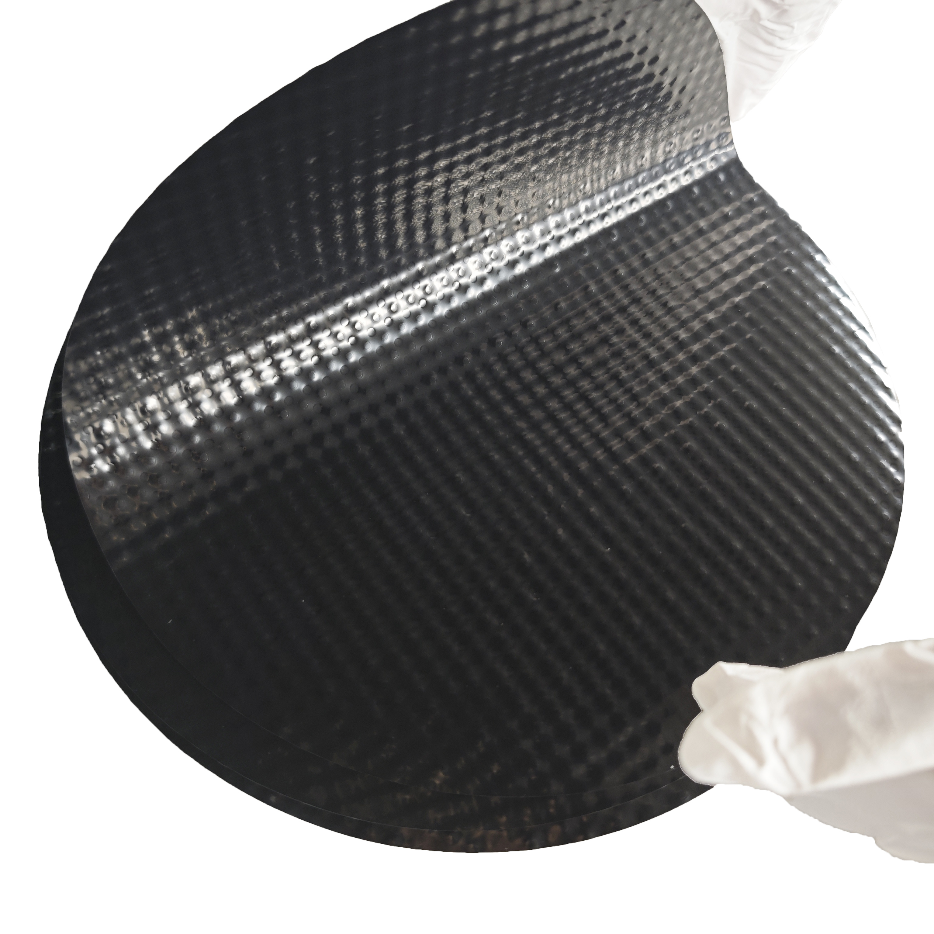
Protective pads offer vital mechanical cushioning for brittle semiconductor materials. Silicon possesses a Mohs hardness of 7. It is exceptionally hard but highly prone to shattering. Embossed or smooth textures actively absorb harmful shock and vibration. They minimize abrasive stress during challenging inter-facility transport. A proper ESD wafer pad physically isolates fragile die surfaces from harsh external vibrations.
Charge dissipation must be carefully controlled across the fab environment. Direct or rapid grounding is extremely dangerous for bare silicon. Resistance below $10^4$ ohms creates high conductivity. This rapid electrical discharge can instantly trigger a destructive Charged Device Model (CDM) event. Sudden sparks easily melt microscopic gate oxides.
Instead, engineered pads target a very specific dissipative sweet spot. They maintain a surface resistivity strictly between $10^5$ and $10^{11}$ ohms. This ideal resistance slows the electrical current safely. It remains conductive enough to prevent hazardous charge accumulation entirely.
Advanced packaging techniques demand flawless wafer edges today. Minimizing physical defects at the wafer bevel is absolutely critical. Downstream processes like 3D NAND stacking require absolute physical integrity. Hybrid bonding processes also fail quickly when edge roll-off or micro-chipping occurs during prior transit steps.
Comparison of Surface Resistivity in Wafer Handling | |||
Material Classification | Surface Resistivity (Ω) | CDM Risk Level | Primary Fab Application |
|---|---|---|---|
Conductive | < 104 | Very High | Rapid machine grounding |
Dissipative | 105 to 1011 | Low | Direct contact carrier pads |
Insulative | > 1012 | High (ESA Risk) | Avoid in cleanroom environments |
Selecting the right base polymer requires careful operational consideration. You must balance strict cleanroom requirements against your chosen mechanical handling methods. Two primary polymer materials currently dominate the market.
Polyethylene provides a softer, highly flexible structure. It naturally offers excellent impact resistance against sudden drops. You will find a PE wafer pad ideal for manual handling environments. It delivers extreme shock absorption under pressure. This makes it perfect for long-distance shipping operations. It reliably excels in any application requiring maximum physical cushioning.
Polystyrene delivers much higher rigidity and superior overall flatness. It features a noticeably lower friction coefficient. A high-quality PS wafer pad is best suited for automated handling equipment. Vacuum wands and robotic arms require this exact dimensional stability. Rigid materials prevent pad sagging inside standard cassettes. PS ensures seamless integration into modern, highly automated production lines.
To choose confidently between these two materials, evaluate your specific operational needs:
Assess your primary transport method. Manual handling strongly favors the flexibility of PE.
Review your automation integration. Robotic loading systems operate best alongside rigid PS.
Determine your transit distance. Long international hauls generally require greater shock absorption.
Analyze your dimensional tolerances. Strict cassette clearances often necessitate PS flatness.
You must actively avoid topically treated materials. These cheap anti-static agents lose efficacy over time. They also fail completely under low humidity conditions. Instead, specify permanent structurally modified polymers. Carbon-loaded or intrinsically dissipative plastics provide lasting protection. A permanent anti-static wafer pad maintains its resistance rating indefinitely.
Non-dusting performance is an absolute requirement. The material must never shed loose particles under physical friction. You must thoroughly validate cleanroom compatibility beforehand. The protective pad itself cannot become a new contamination source. Industry standards like ANSI/ESDA and SEMI strictly enforce these particulate-free mandates.
Dimensional customization plays a crucial role in safe edge protection. Pads must precisely match standard semiconductor wafer diameters. Common sizes include 6-inch, 8-inch, and 12-inch formats. Accurate sizing maintains vital edge-only clearance zones. These zones typically require 2 to 5 millimeters of precise clearance from the edge. They must also fit seamlessly into standard Front Opening Unified Pods (FOUPs).
Finally, outgassing and chemical inertness demand strict continuous verification. Low outgassing properties prevent Airborne Molecular Contamination (AMC). Unwanted chemical transfer onto the wafer surface ruins sensitive photolithography steps. Prolonged storage requires highly inert polymers to maintain pristine substrate conditions.
Environmental humidity directly impacts static neutralization rates. Even premium dissipative materials require adequate atmospheric moisture. Fab relative humidity (RH) should always be maintained above 40 percent. This specific moisture level reliably supports the safe, continuous dissipation of surface charges.
You must actively audit your full packaging loop. A premium pad becomes completely ineffective if misused. Placing it inside an insulative, highly-charging plastic container destroys its value. Ensure seamless integration alongside certified ESD-safe cassettes. Workstations and transit handling equipment must also maintain proper grounding protocols.
Testing and validation prevent massive yield disasters. Always request physical samples before bulk procurement. Conduct thorough surface resistivity audits using standard megohmmeters. Validate particle generation rates under simulated transit conditions. Rigorous empirical testing guarantees your protective investment actually secures your sensitive silicon.
Upgrading to engineered ESD wafer pads is a negligible cost compared to the yield loss associated with wafer edge defects, ESA-induced contamination, and latent device failure. Protecting your silicon investment requires comprehensive physical and electrical strategies.
Audit your current transit consumables immediately to identify highly insulative plastics touching bare substrates.
Map out your exact automation requirements to choose effectively between flexible PE and rigid PS materials.
Establish strict surface resistivity benchmarks ($10^5$–$10^{11}$ ohms) when evaluating new vendor materials.
Demand non-dusting certificates and run internal particle generation tests before full fab deployment.
A: Typically in the dissipative range of $10^5$ to $10^{11}$ ohms to prevent both static buildup and rapid CDM discharges.
A: Standard plastics might, but specialized anti-static wafer pads are engineered with non-dusting materials specifically for cleanroom environments.
A: A "separator" is a generic term for any physical divider, whereas an "ESD pad" specifies a separator that actively manages electrostatic dissipation.
A: Their reusability depends heavily on your specific fab protocols. Physical deformation and micro-particulate buildup severely limit their lifespan. Advanced node manufacturing generally treats these pads as single-use items. Less sensitive applications might permit limited reuse following rigorous cleaning and strict particle inspection procedures.
