
- All
- Product Name
- Product Keyword
- Product Model
- Product Summary
- Product Description
- Multi Field Search

 |


| Quantity: | |
|---|---|
PS WAFER PAD/Wafer Separator/ Wafer Spacer/Wafer Pad
product model:JH5063
The WAFER PAD A wafer pad is also called an anti-static accumulation pap, a silicon wafer paper, a buffer pad in a semiconductor wafer box, A solar wafer buffer pad, a semiconductor wafer box inner pad, a PCB buffer pad, a conductive spacer, a black wafer spacer, an anti-static wafer spacer, a conductive wafer spacer, a circular wafer spacer, a wafer square, and the surface treatment process thereof is also called an anti-static black embossed wafer pad, an embossed wafer square, and the like.
This product is made of permanent conductive or anti-static film through hot-pressing, die-cutting. Film surface can be made smooth, can also be made according to the requirements of a variety of patterns. The product can be made into any size and shape according to the requirements, and the finished product has excellent dimensional stability, clean appearance, no powder falling and no dust. Protruding patterned wafer pads can not only effectively prevent the product from electrostatic damage, but also play a certain role in cushioning.
Such products are widely used in chip manufacturing, packaging and other enterprises TFT-LCD, solar cell wafer, wafer, solar silicon wafer packaging of multi-monocrystalline silicon wafer.
The main technical parameters:
Model | Material | Size(in) | Diameter(mm) | Surface Resistance(Ω/Sq) | Thickness (μm) | Surface |
JH5063 PE | PE | 4/5/6/6.5/7 /8/10/11/12 /14/15/16/ Customized | 100/125/150(152,155)/ 165/180(178)/200(203)/ 254/275/300(299,305)/360 /380(390)/400/Customized | 10K-1M/ 1G-100G | 100/ Customized | Embossed with dots/Smooth/Customized |
JH5063 PS | PS | 4/5/6/6.5/7 /8/10/11/12/ 14/15/16/ Customized | 100/125/150(152,155)/ 165/180(178)/200(203)/ 254/275/300(299,305)/360 /380(390)/400/Customized | 100K-1G | 100/ Customized | Embossed with squares or dots/smooth/Customized |
Question 1: What is the core role of HAOUGER's Wafer Pad in the semiconductor and solar wafer industry chain? What are the competitive advantages of the manufacturer compared to similar suppliers?
Answer: - Core role: It plays a dual role of "protection and separation" in the industry chain — through anti-static properties, it prevents wafers from adsorbing dust due to static electricity or suffering electrostatic breakdown; through buffering properties, it reduces collision damage during wafer transportation/storage; and through the interval design, it realizes the separate storage of multiple wafers to prevent friction and scratches between wafers. Competitive advantages: ① Experience advantage: The manufacturer has rich experience in the production and application of wafer pads, and the product adaptability is stronger; ② Customization advantage: It supports full-dimensional customization of shape, diameter, and surface pattern to meet personalized needs; ③ Cost-performance advantage
Question 2: How long is the validity period?
Answer: It is made of permanent conductive/antistatic film material, with no clear attenuation period for its antistatic performance. Under regular storage conditions (avoiding high-temperature and strong corrosive environments) and normal frequency of use, it can maintain stable performance for 3-5 years without the need for additional treatment.
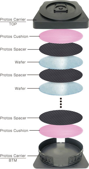
Question 3: What are the installation and usage methods?
Answer: No additional tools are required; simply stack the wafer pads and wafers alternately in the wafer box. When the embossed side faces the wafer, the buffering effect is better; when the smooth side faces the wafer, it is more convenient to pick and place. You can choose according to actual needs.
Multi-specification Wafer Adaptation Case of IC Design Company
Customer Background: A small and medium-sized IC design company, mainly engaged in consumer electronic chips (such as MCU), involving multiple specifications of wafers (4-inch, 6-inch, 8-inch), with small purchase quantities (50-100 pieces per specification) and flexible demands.
Core Pain Points: Multiple specifications of wafers require adaptation to different wafer boxes. The original supplier has a high minimum order quantity (500 pieces per specification) and a long customization cycle (15 days); and the electrostatic protection requirements for different specifications of wafers are different (low resistance / medium resistance), making it difficult to find a one-stop solution.
Product Solution: Provide a "standardization + customization" combination solution. Standard sizes of 4/6/8 inches are available in stock (minimum order quantity 100 pieces), and special sizes (such as 6.5 inches) are delivered within 7 days through customization; recommend materials based on wafer types (PE low-resistance model for logic chips, PS medium-resistance model for analog chips); unified packaging, marking specifications and usage scenarios, facilitating management.


