
- All
- Product Name
- Product Keyword
- Product Model
- Product Summary
- Product Description
- Multi Field Search

 |


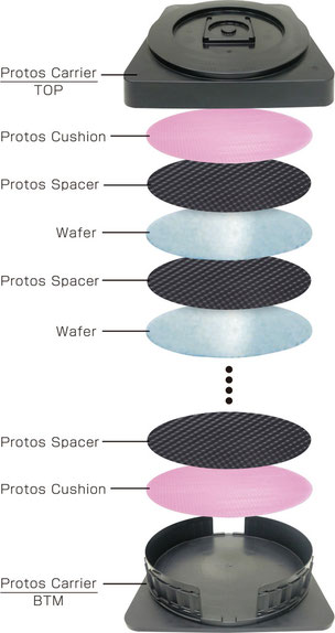
•Wafer PAD
product name:
Wafer Separator/ Wafer Spacer/Wafer Pad
product model:JH5063
Product Description:
Wafer pads, also known as wafer spacer or wafer separator, is made of conductive and anti-static film through hot pressing and die cutting. Various patterns, sizes and shapes can be customized, the finished products have excellent dimensional stability, and the appearance is neat and does not drop powder or dust.
Application:
• Wafer separators are widely used in the separate packaging of multi/monocrystalline silicon wafers such as solar cells, wafers, and solar silicon wafers.
Product Feature
·PS material
·Various patterns, sizes and shapes can be customized
·Stable anti-static
·Embossed surface
·Easy to Grasp
·For cleanroom
Product Specification
Model | Material | Size(in) | Diameter (mm) | Surface Resistance (Ω/Sq) | Thickness (μm) | Surface |
| JH5063PE | PE | 4/5/6/6.5/7/8/10/11/12/14/15/16/Customized | 100/125/150(152,155)/ 165/180(178)/200(203)/ 254/275/300(299,305)/360 /380(390)/400/Customized | 10K-1M/ 1G-100G | 100/Customized | Embossed with dots/Smooth/Customized |
JH5063PS | PS | 4/5/6/6.5/7/8/10/ 11/12/14/15/16 | 100/125/150(152,155)/ 165/180(178)/200(203)/254/275/300(299,305)/360 /380(390)/400/定制 Customized | 100K-1G | 100/120/160 Customized | Embossed with squares or dots/smooth/Customized |
Advantages of HAOUGER Embossed Semiconductor Wafer separators for Back End :
·Embossed Semiconductor Wafer separators for Back End are widely used in the separate packaging of multi/monocrystalline silicon wafers such as solar cells, wafers, and solar silicon wafers.
·HAOUGER Embossed Semiconductor Wafer separators for Back End can be customized with shapes, diameters, surface patterns.
·HAOUGER has plenty of experience in making and using wafer separators, we provide products with high quality, low price and short lead time.


