
- All
- Product Name
- Product Keyword
- Product Model
- Product Summary
- Product Description
- Multi Field Search

Views: 0 Author: Site Editor Publish Time: 2026-08-14 Origin: Site


In advanced semiconductor manufacturing, the journey from fab to final assembly carries immense mechanical, electrostatic, and chemical risks. A single microscopic flaw can ruin an entire high-value production run. Unfortunately, the temporary interleaving materials used to protect sensitive substrates are often treated as an afterthought. Relying on substandard interleaving layers inevitably leads to catastrophic micro-scratches, foreign object debris (FOD), or silent electrostatic discharge (ESD) failures. You simply cannot afford unpredictable yield losses during sensitive packaging phases. This guide provides a purely objective, metric-driven framework for evaluating and shortlisting protective components specifically for ISO-certified cleanroom environments. You will learn how to identify the precise physical, electrostatic, and chemical requirements needed to fully secure your operations. Let us explore how to engineer uncompromising safety into every critical transport step.
Selecting a wafer spacer requires balancing physical protection (TTV, scratch resistance) with stringent contamination control (low outgassing, trace metal limits).
Standard plastics are fundamentally incompatible with semiconductor packaging; baseline materials must include HDPE (like Tyvek), pure Polystyrene (PS), or advanced inherently conductive polymers.
Not all ESD protection is equal—evaluating the exact mechanism (carbon vs. surfactant vs. conductive polymer) is critical to preventing secondary particle shedding or chemical bleed-out.
Compliance with testing standards like EIA STD 541, RoHS, REACH, and ISO 14644-1 is non-negotiable for supply chain security.
Modern semiconductor substrates present a unique material paradox. Silicon boasts a Mohs hardness of 7, making it remarkably hard. However, it cleaves effortlessly along crystallographic planes under mechanical stress. When you design packaging workflows, your chosen wafer spacer must support the substrate evenly. It must never apply concentrated pressure to the highly critical 2–5mm edge exclusion zone. Minor edge stress often propagates into catastrophic die cracks during subsequent processing steps.
Beyond physical fragility, manufacturers face insidious, invisible threats from substandard packaging.
Trace Metal Contamination: Standard commercial plastics readily transfer trace metals onto silicon surfaces. Advanced node architectures require detection thresholds down to 10⁶–10⊃1;⁰ atoms/cm². Contaminated spacers will fail these stringent VPD-ICP-MS testing standards.
Outgassing (VOCs): Standard polymers degrade over time. They release volatile organic compounds (VOCs) into the micro-environment. These compounds form an invisible "organic fog" over the wafer surface. This fog directly causes photolithography defects and severe packaging delamination later in production.
Vacuum Handling Damage: Automated fabs rely on vacuum wands and robotic handlers. Spacers utilizing chemical binders risk sticking to wafers or shedding particulate matter under vacuum manipulation. This disrupts automated handling and introduces severe foreign object debris (FOD).
Common Mistake: Many engineers assume visual cleanliness equates to cleanroom compatibility. Always remember that the most damaging contaminants—VOCs and trace metals—remain invisible to optical inspection systems.
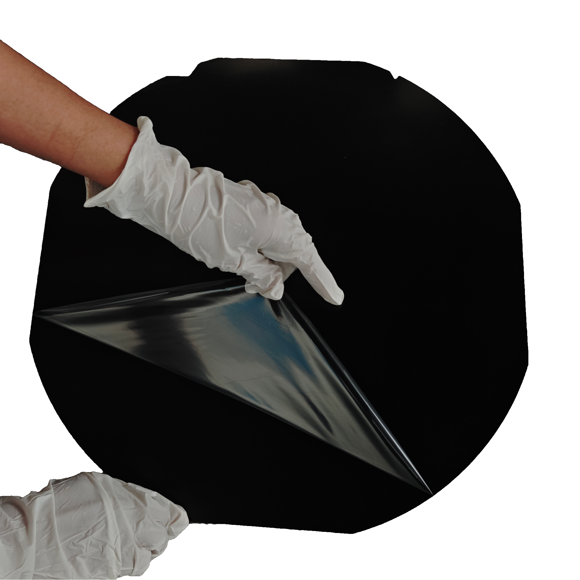
Semiconductor packaging explicitly demands specialized material formulations. You cannot retrofit standard consumer plastics for cleanroom applications. Below, we examine the three dominant material baselines utilized in modern fabs.
Manufacturers create Tyvek by flash-spinning high-density polyethylene (HDPE). This process eliminates the need for chemical binders.
Characteristics: It offers exceptional tear resistance, lint-free properties, and high porosity. It contains no plasticizers.
Use Case: HDPE serves brilliantly inside horizontal shippers. It withstands vacuum handling protocols easily and prevents physical friction damage during transit.
Pure polystyrene provides an excellent balance of rigidity and surface smoothness.
Characteristics: It comes in rigid or semi-rigid formats. It delivers outstanding dimensional stability and ensures concentric separation between layers.
Use Case: You will typically deploy a PS wafer separator for heavier substrates. Environments demanding a highly flat, low-friction protective layer benefit immensely from pure polystyrene.
High-end packaging requires next-generation polymer science. Inherently static-dissipative polymers represent the peak of material engineering.
Characteristics: These custom blends offer high purity. They withstand extreme operational temperatures, ranging from 150°C to 315°C.
Use Case: Engineers select these materials for silicon carbide (SiC) power devices or ultra-thin wafers (<50 µm). They guarantee thermal stability and zero particle shedding.
Baseline Material Comparison Table | |||
Material Type | Primary Advantage | Optimal Use Case | Temperature Limit |
|---|---|---|---|
HDPE (Tyvek) | Tear resistance, no binders | Horizontal shippers, vacuum compatibility | ~118°C |
Polystyrene (PS) | Dimensional stability, flatness | Heavy substrates, concentric separation | ~90°C |
Conductive Polymers | Inherently static dissipative | SiC devices, ultra-thin substrates | 150°C – 315°C |
Procuring reliable semiconductor wafer consumables requires a strict evaluation methodology. You must measure performance across three non-negotiable dimensions.
Any interleaving material entering the fab must meet ISO 14644-1 Class 4 to 6 limits. You must verify "no powder shedding" characteristics under friction. When automated arms slide wafers into cassettes, micro-abrasion occurs. Inferior materials will shed thousands of particles per square centimeter. Insist on optical particle counter data proving structural integrity during dynamic friction tests.
Modern packaging often processes extremely thin substrates. For thin-wafer handling (<50 µm), Total Thickness Variation (TTV) becomes a critical metric. Your interleaving layers must maintain a strictly controlled TTV, often ≤15 µm. Furthermore, general thickness tolerances must stay within ±5–10 µm. Excessive variation induces localized stress. This stress warps fragile wafers during long-distance transit.
Chemical stability matters just as much as physical form. Spacers must carry certified amide-free and silicon-free designations. Commercial plastics frequently utilize topical surfactants and slip agents to improve mold release. In a cleanroom, these agents inevitably migrate onto the wafer surface. They poison sensitive layers and cause catastrophic failures during bonding or deposition steps.
Electrostatic discharge presents a silent, highly destructive threat to advanced nodes.
The ESD Risk: Humans cannot perceive static charges below approximately 3000V. However, modern gate oxides can rupture from less than 50V. Therefore, deploying a highly reliable conductive wafer spacer is mandatory for yield protection. You must actively safely drain accumulated charge away from the device.
Comparing Anti-Static Technologies:
You have three primary technology paths for ESD protection. Each carries distinct operational tradeoffs.
Topical Surfactants: These represent the cheapest option. Unfortunately, they depend heavily on ambient cleanroom humidity to function. Fabs strictly restrict humidity to 45-50%. Under these dry conditions, surfactants dry out entirely. They lose efficacy and bleed chemical residues directly onto the wafer.
Carbon-Loaded Materials: Carbon doping provides stable, permanent conductivity. It ignores humidity levels completely. However, carbon-loaded plastics inherently suffer from particle shedding. This phenomenon, known as carbon sloughing, directly causes unacceptable FOD inside the cassette.
Intrinsically Conductive Polymers: Polypyrrole-based polymers represent the optimal engineering choice. They deliver the essential "3Cs": Conductive (permanent, humidity-independent dissipation), Clear (allowing automated optical inspection), and Clean (zero carbon shedding, zero outgassing).
When engineering an ideal anti-static wafer spacer, target a steady surface resistance between 10⊃3; and 10⊃1;⊃1; Ω/sq.
ESD Technology Summary Chart | |||
Technology Type | Conductivity Source | Cleanroom Suitability | Primary Drawback |
|---|---|---|---|
Topical Surfactants | Moisture absorption | Poor (Fails in dry fabs) | Chemical bleed-out, outgassing |
Carbon-Loaded | Carbon black network | Moderate (Requires cleaning) | High particle shedding (sloughing) |
Conductive Polymers | Intrinsic polymer chain | Excellent (ISO Class 4-6) | Higher initial material cost |
Your protective layers must seamlessly integrate with existing automated infrastructure. Physical shape determines mechanical success.
Shape and Die-Cut Precision:
Round Formats (2-12 inch): Round geometries remain standard for wafer cassettes, single-wafer containers, and coin stack applications. A precisely cut wafer box spacer ensures concentric separation. It strictly protects fragile edges from bumping against container walls.
Square/Custom Formats: Engineers utilize square formats in specific dicing, frame carrier, or sensor production configurations. Here, you must implement corner stress-reduction designs. Sharp internal corners concentrate stress and cause substrate micro-cracks.
Automation Compatibility:
Modern fabs run on SCARA robots and precise vacuum manipulation tools. You must ensure spacer thickness and weight parameters match robotic tolerances. If an interleaving layer weighs too little or sticks due to static, robots suffer "double-picking" errors. This jams Front-Opening Shipping Boxes (FOSBs) and Front-Opening Unified Pods (FOUPs). Precise dimensional stability eliminates handling bottlenecks.
Selecting a supplier requires rigorous auditing. Never rely on superficial marketing brochures.
Require Hard Data over Marketing Claims: Demand comprehensive testing documentation. A qualified vendor will readily supply surface resistance curves demonstrating compliance with EIA STD 541. They must provide localized particle count data and formal outgassing mass loss reports.
Evaluate Compliance: A credible vendor must provide RoHS and REACH compliance certificates. These documents explicitly prove the absence of Substances of Very High Concern (SVHC). Validating this documentation secures your downstream supply chain against sudden regulatory blocks.
Test for Target Contaminants: Always conduct independent sample testing before mass rollout. Use optical particle counters to verify resistance to friction-induced FOD. Utilize ATD-GC-MS (Automated Thermal Desorption Gas Chromatography-Mass Spectrometry) for organic residue verification. This protocol uncovers any hidden VOC threats before they enter your pristine cleanroom.
Selecting the correct protective materials remains a fundamental exercise in risk mitigation. You cannot cut corners on temporary interleaving layers without exposing your operations to immense vulnerability.
Actionable Takeaways & Next Steps:
Audit Existing Materials: Immediately cross-reference your current packaging layers against ISO 14644-1 and EIA STD 541 requirements.
Reject Standard Plastics: Transition exclusively to pure HDPE, polystyrene, or intrinsically conductive polymers to eliminate VOC and trace metal threats.
Demand TTV Certifications: For thin wafers, insist on TTV metrics ≤15 µm to prevent stress-induced warpage during transport.
Validate ESD Mechanisms: Avoid topical surfactants. Prioritize polypyrrole-based polymers for permanent, clean static dissipation.
Request Lab Kits: Encourage your engineering teams to request material sample kits. Run internal ATD-GC-MS and optical particle counting tests before committing to a vendor.
A: The optimal range is typically between 10⊃3; to 10⊃1;⊃1; Ω/sq, ensuring rapid but controlled static dissipation without acting as a direct conductor that could cause a hard short.
A: Standard commercial anti-static plastics use chemical surface agents that depend on atmospheric moisture to work. In a controlled fab environment, they dry out, lose efficacy, and off-gas contaminants onto the wafer.
A: For handling highly sensitive thin wafers, premium spacers generally maintain a TTV of ≤15 µm and a strict thickness tolerance of ±5 µm to ensure uniform load distribution during transit.
