- All
- Product Name
- Product Keyword
- Product Model
- Product Summary
- Product Description
- Multi Field Search
•Wafer PAD
product name:
Wafer Separator/ Wafer Spacer/Wafer Pad
product model:JH5163
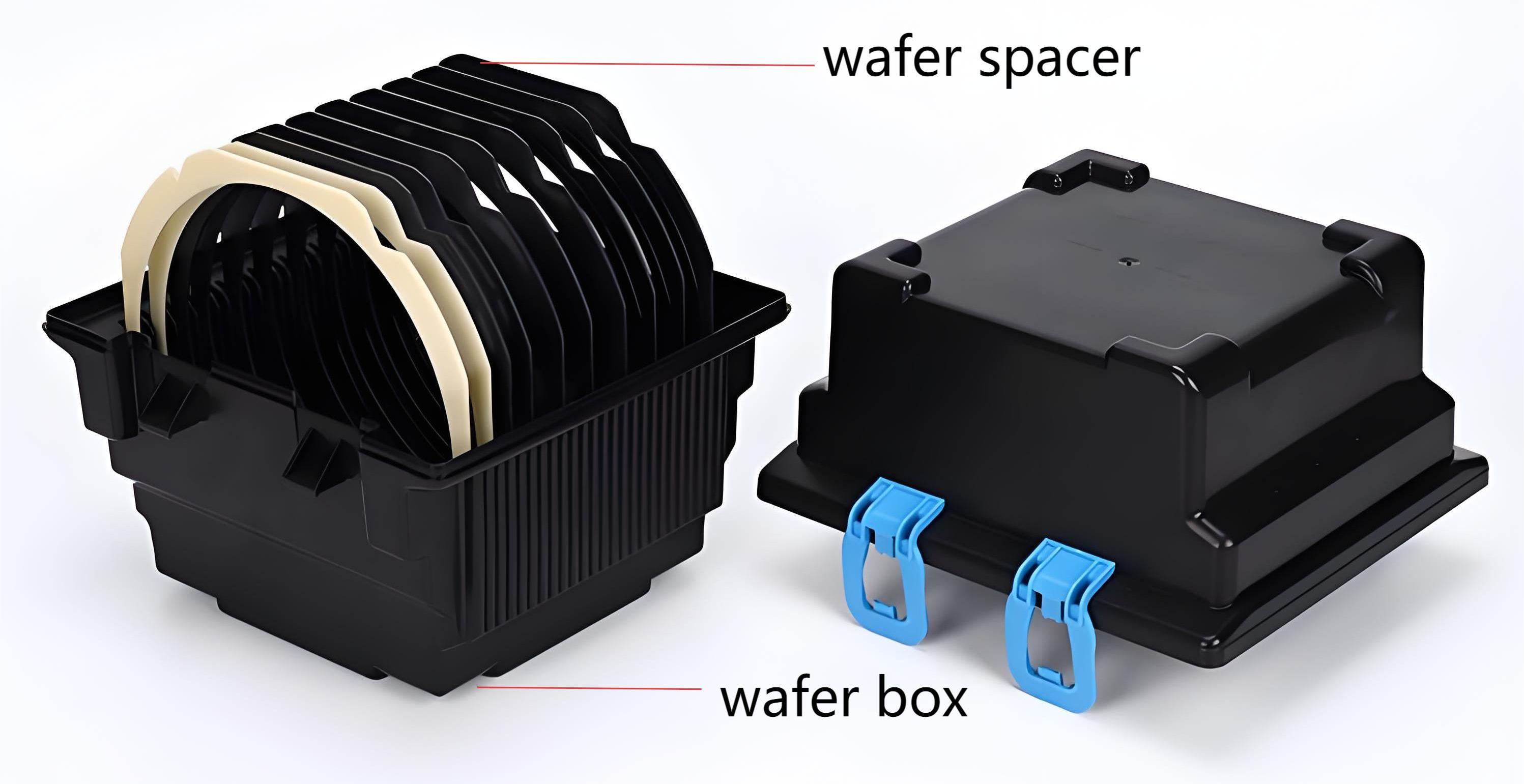
Wafer spacer, also known as the inner spacer of the wafer box, is made by hot-pressing and shaping conductive and anti-static plates and then die-cutting them. It can be customized in various sizes and shapes.
The finished products have excellent dimensional stability, a clean appearance, no powder shedding and no dust emission. Such products are widely used in solar cell, wafer, solar silicon single crystal silicon slice of separate packing.
Product Feature
·PS material
·Various patterns, sizes and shapes can be customized
·Stable anti-static
·Embossed surface
· For cleanroom
Product Specification
Model | Material | Size (in) | Diameter (mm) | Surface Resistance (Ω/Sq) | Thicknes(mm) | Surface |
JH5063PS | PS | 4/5/6/6.5/7/8/10/ 11/12/14/15/16/customized | 100/125/150(152,155) /165/180(178) /200(203)/254/275/300(299,305)/360 /380(390)/400/ Customized | 10K-1M/1G-100G | 0.8/1.2/1.8/2/ Customized | Glossy/Customized |

The core function of PS wafer spacers lies in:
Physical protection: Absolutely prevents scratches caused by direct contact between wafers.
Electrostatic protection: Through anti-static treatment, static charges are dissipated to prevent ESD damage and particle adsorption.
Buffering and shock absorption: Absorb the vibration and shock energy during transportation and operation.
Maintain cleanliness: Reduce particle generation and migration, and protect the wafer surface.
Auxiliary operation: Ensure that the wafers are correctly positioned within the box to facilitate automated handling.
Advantages of HAOUGERPS Small Conductive Wafer separators
·PS Small Conductive Wafer separators are widely used in the separate packaging of multi/monocrystalline silicon wafers such as solar cells, wafers, and solar silicon wafers.
·HAOUGERPS Small Conductive Wafer separators can be customized with shapes, diameters, surface patterns.
·HAOUGER has plenty of experience in making and using wafer separators, we provide products with high quality, low price and short lead time.